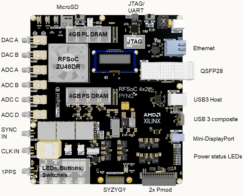
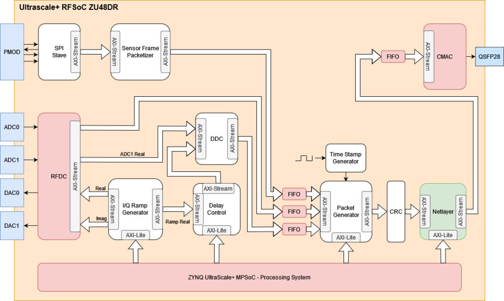
FPGA Overview: RFSoC 4×2 Kit from XilinxADCs with 5GSps and 14-Bit resolution.DACs with 10GSps and 14-Bit resolutionQSFP28 interface for up to 100GB/s data transmissionConfiguration via PS using Pynq (Quad Core ARM Cortex-A53 & Dual Core ARM Cortex-R5F)GPIOs via SYZYGY and Pmod interface Block Diagram: Processing system:configure the signal processing chainI/Q ramp generator: creates FMCW rampes with customizable parametersRFDC: analog to AXI-Stream / AXI-Stream to analogDelay control:compensates delay of the RFDCDDC:digital down converter mixes Rx and Tx and decimates by 32Packet Generator:inserts meta data at the beginning of the packet and forwards data to CRCCRC:calculates checksum for data integrityNetlayer:stores the data into UDP, IP, Ethernet frameCMAC:signalling for 100GbESPI Slave:receives data from companion boardSensor Frame Packetizer:adepts received data to desired format SPI protocol: Timestamped sensor data from companion board developed by HGB bachelor projectUp to 50 MHz SPINew data every 1 msData integrity with CRC